Electronics Production
PCB Fabrication
Printed Circuit Board or PCB are used to configure all the electronic components of a device together. The traces of a circuit board connects all of the electrical signals from one junction to another. In our last module, we used an Arduino to help us assemble our circuit. Now going up a level higher, we learnt how to build our own PCB. This means we have the flexibilty to design and customise our microcontroller board for better product integration.

A PCB of an electronic device.
There are a few methods of pcb manufacturing out there. Here, we will be only focusing on milling them on a CNC machine. What is great about machining your PCB is that it does not create toxic waste like the lithography process or other method that uses chemical.
This are generally the steps on how to create your custom PCB:
Step 1: CAD
To design our schematics, we are using EAGLE as our software. EAGLE lets PCB designers make circuit boards by editing their schematics before printing it out. You can check out more of this topic on my Electronics Design page.
Step 2: CAM
After designing the circuit, we will have to generate the G-code based on the board layout. G-code is the language of CNC machines. It instructs the machine on how and where to move. There are two ways to go about this.
- Using mods
- Prepare image file in png.
- To set parameters: right click to begin > programs > open programs > G-code: mill 2D pcb.

Mods Community interface.
- Using EAGLE
- Generate using EAGLE’s pcb-gcode ULP (User Language Programme).
- Set parameters.
I demonstrated this in Electronics Design page.
Before milling, we can check the simulation with CAMotics.
Step 3: Milling
After generating the G-code, you can now prepare the board for milling. You should have 2 files ready to load; etch(traces) and mill(outline). Familiarise yourself with the CNC machine you are using. In Fablab SP, we are using the STEPCRAFT 420 and UCCNC for the CNC control software.
Some G-code lines that are useful to know (example):
F60.000 - Move at a feed rate of 60
Z-0.050 - Z-coordinate depth of -0.05
X10.903 - Move to this X-coordinate
Y1.9556 - Move to this Y-coordinate
Step 4: Assembly
With your freshly milled pcb board, you can now solder the components together. Refer to your schematic to assign the parts and orientation correctly. Use a multimeter to inspect for shorts between VCC and GND.
How to inspect continuity between GND and VCC
- Measure between GND pins of ATtiny85 and ISP header. Multimeter should beep and read 0 Ohm.
- Measure between VCC pins of ATtiny85 and ISP header. Multimeter should beep and read 0 Ohm.
- Measure between VCC and GND pins. Multimeter should not beep and read OL (overload). Overload means there is no connection (short circuit).
- To check LED working, check circuit between VCC and GND. LED should light up.
Assignment: Make an in-circuit programmer by milling and stuffing the PCB
Building a FabTinyISP Programmer
ISP (In-system Programming, also called in-circuit serial programming) Programmers is used to program microcontrollers while being installed in a complete system, rather than requiring the chip to be programmed prior to installing it in the system. This allows the microcontrollers to be re-programed without being removed from the target board.
Here are some articles explaining more about it:
https://en.wikipedia.org.
http://www.ethernut.de.
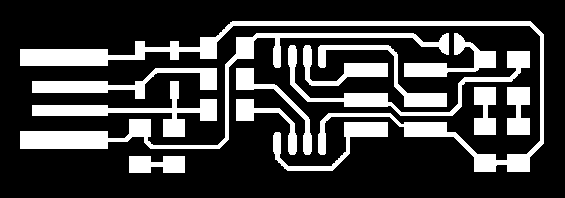
The PCB that i’m making is based on the Brian’s FabTinyISP. This board was specifically designed to be made in a Fablab. More about it here
First, i save the png files in my computer.

Traces 1000 dpi 
Outline 1000 dpi
I will be generating the G-code in mods community. Import the traces file and set the parameters. This is the recommended setting for STEPCRAFT 420.


Setting up parameters in Mods Community
Then, click the Calculate button to download the G-code. You will also be able to see the toolpath. Do the same for the Outline with its correct settings. These are the files that I generated. It should end with .nc.
fts_mini_traces.png.nc
fts_mini_cut.png.nc
Now, you will need to prepare a few things at the cnc milling station. They are:
- Files ready in a thumbdrive
- Blank circuit board. We use copper clad plate.
- Bits and end mills
- Double-sided tape and masking tapes
- Wrench to tighten spindle
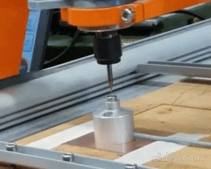
Hold down the copper plate on the MDF board. I will be taping underneath with a double-sided tape and tape on its side to secure it down. Then, attached the end mill. Make sure it is secured tight.

My attached copper baord

0.1mm 30 deg V bit for etching

0.8 mm end mill for cutting outline
Load the file in UCCNC. Set the X and Y origin. Then calibrate the Z-axis. Select Start cycle.
Calibrating Z-axis on a flat surface with a touch plate

Milling in operation
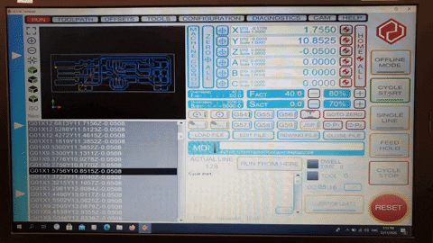
What you should see on the laptop
To cut the outline, leave the origin point at the same place. Calibrate the Z-axis again. And change the bit to 0.8mm end mill.
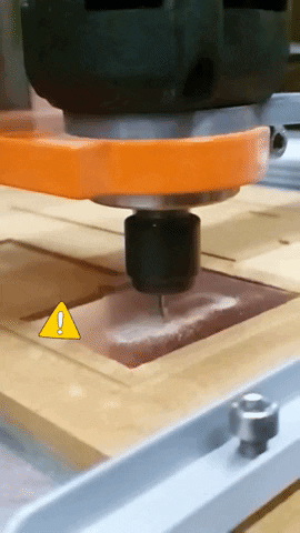
During the milling, the end mill broke apart. I realised the pressure from the spinning spindle could break the bits. Therefore always give attention to your milling process. We could control the speed setting to prevent it from breaking. Immediately stop operation if it happens.

Burr. Since the end mill was not very sharp. The outcome of my milling has a lot of burr. I sand lightly on the surface of the rised edge. Use the finest sand paper grit available. Be careful not to remove the copper traces in the process.
I prepared the components and start soldering.

At the soldering workstation
I refer from Brian’s board image and schematic to determine where the components are placed. This is to take note that I have placed them in the right orientation (for ATtiny85, LED and Zener diode).


This is my soldered ISP board. I may need to work on my soldering skill but so far all of the connections are fine. Next, I will need to program this board for it to become an AVR programmer.

My completed Board
Programming my ISP board
Software Installation
To set up my development environment, i installed the following softwares.
- Git
- Atmel GNU Toolchain
- GNU Make
- Avrdude
- Zadig
Avrdude and GNU Make installer can be downloaded from Brian’s page. Then I update my path on Windows Control Panel> Advanced System Setting > Environment Variables

To check everything is installed, run Git Bash and type:
- make -v
- avr-gcc –version
- avrdude -c usbtiny -p t85

nur_a@DESKTOP-MGQR7F7 MINGW64 ~
$ avrdude -c usbtiny -p t85

avrdude.exe: initialization failed, rc=-1
Double check connections and try again, or use -F to override
this check.

avrdude.exe done.  Thank you.
Initialization failed “This means that avrdude successfully found your programmer, but failed to talk to a target board (expected because we don’t have anything conencted to the programmer right now.” -Brian’s page
Then, download the firmware source code. Again, find it on Brian’s page. Extract and edit the makefile. Type in the correct MCU. 

